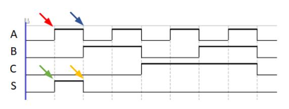
The objective is to create the following digital circuit in LTSpice using MOSFET transistors:

We have a few requirements in order to do this:
First, we have to create a .cir file so we can begin describing our gates. Inside of that file, we're going to include the AMS library with .include ams35ps.lib.
Now, we need a power source for the whole circuit. We can add that with <name> <node+> <node-> <value>. Let's add a 3.3V power source with VDD VDD 0 3.3V.
For handling the inputs, we're going to add 3 pulse-type power sources. We can add them with VC C 0 PULSE(0v 3.3v 0ns 0.1ns 0.1ns 1ns 2.2ns).
Note that for the next 2 we have to double the period (last parameter) so that we can have all possible combinations when running the simulation.
Let's put aside the capacitive load for now, and instead begin building the logic gates. Those are going to be subcircuits inside our file, which we will call later.
A subcircuit has a prototype .subckt <name> <arguments>, followed by the description of the subcircuit, and then an end .ends <name>.
To build our CMOS gates, we can use the following pattern: <name> <drain_node> <gate_node> <source_node> <bulk_node> <type> <W=> <L=>
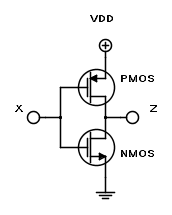
.subckt inv IN OUT VDD
M1 OUT IN VDD VDD MODP W=180u L=0.35u
M2 OUT IN 0	  0	  MODN W=85u L=0.35u
.ends inv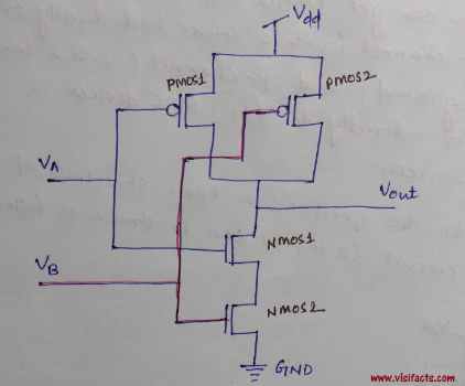
.subckt nand A B OUT VDD
M1 OUT A VDD VDD MODP W=80u L=0.35u
M2 OUT B VDD VDD MODP W=80u L=0.35u
M3 OUT A X   0   MODN W=50u L=0.35u
M4 X   B 0   0   MODN W=50u L=0.35u
.ends nand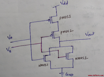
.subckt nor A B OUT VDD
M1 X A VDD VDD MODP W=80u L=0.35u
M2 OUT B X VDD MODP W=80u L=0.35u
M3 OUT A 0   0   MODN W=50u L=0.35u
M4 OUT B 0   0   MODN W=50u L=0.35u
.ends nor
Now that we have all the subcircuits, let's add the capacitive load and then call each subcircuit.
We can add the capacitive load with <name> <node+> <node-> <value>. Let's add a 0.5pf load with C1 OUT3 0 0.5pf.
Next, let's finally call all the subcircuits.
X1 A OUT VDD inv
X2 OUT B OUT2 VDD nand
X3 OUT2 C OUT3 VDD nor
Now all that's left is for us to measure the delays tpLH and tpHL. For that we can use the .measure directive, along with various parameters.
Let's set the simulation time with .tran 0.001ns 8.8ns, end the description with .end and check the waveform we get by running the code.
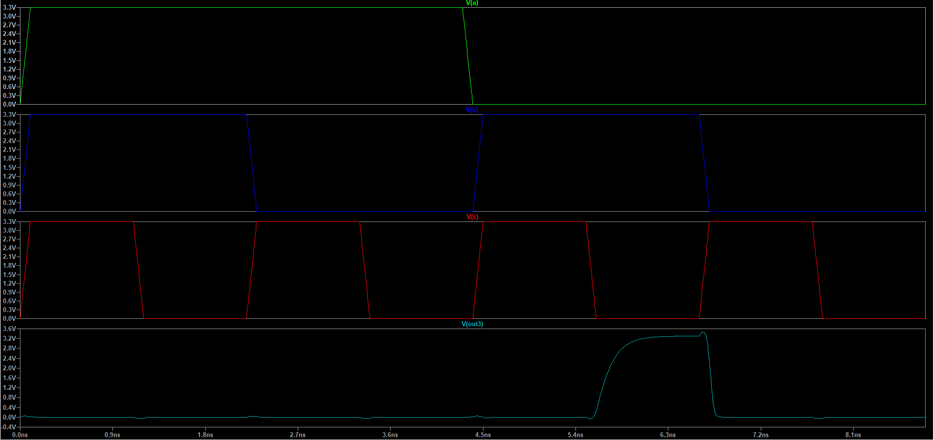
Notice that the output is HIGH when only B is HIGH. That delay on OUT3 between 0 and 3.3v (and 3.3v to 0 as well) is what we want to measure.
So, we can set the trigger at the 3rd fall of the C input to measure tpLH, and at the 4th rise of the C input (or at the 2nd fall of the B input) to measure tpHL.
We also have to specify our target when measuring, that being the 1st rise and 1st fall of the OUT3 output, respectively.
.measure tran delay_tpLH 	trig v(C) val=1.65v fall = 3	targ v(OUT3) val=1.65v rise = 1
.measure tran delay_tpHL 	trig v(C) val=1.65v rise = 4	targ v(OUT3) val=1.65v fall = 1
You can hit CTRL + L, or click View -> SPICE Output Log and see the .log file for more info on the measurements.